RecommendMail Facebook LinkedIn
Electro optical modulators
The integrated optical modulators allow you to influence the amplitude or phase of laser light quickly and with high dynamics.
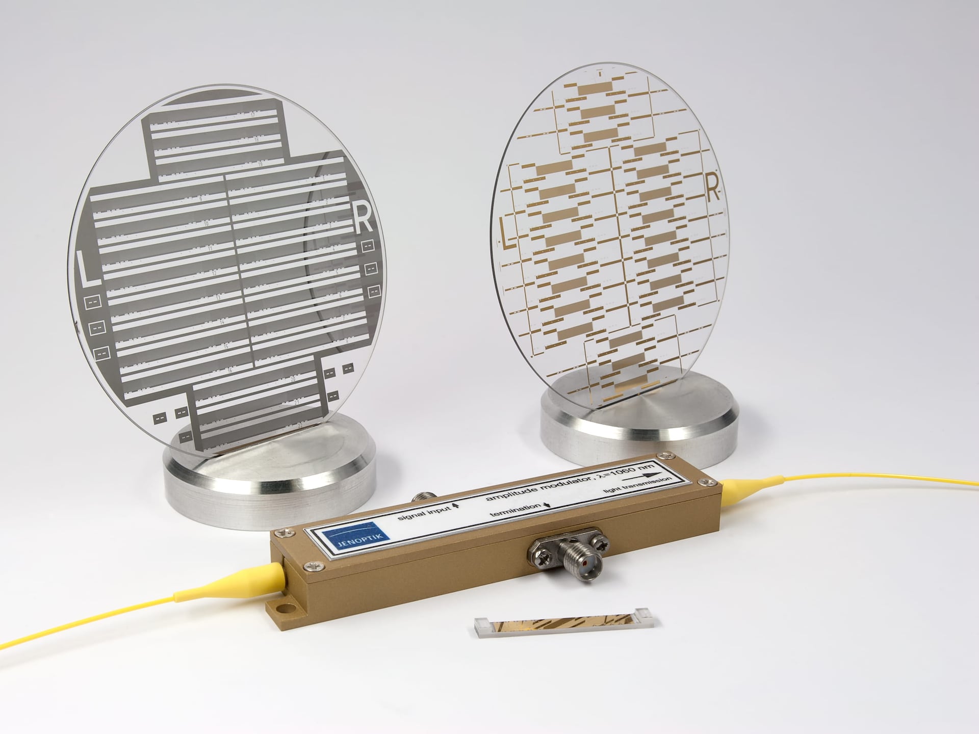
Amplitude modulator, modulator crystal and structured lithium niobate wafers
The fiber-coupled integrated optical modulators from Jenoptik are ideal for the amplitude or phase modulation of laser light. You can cover wavelengths of between 500 and 1.750 nanometers.
The modulators are based on electro-optical crystals and make use of their rapid electro-optical effect. You can use them to influence the phase or amplitude of light up to high modulation frequencies in the gigahertz range. In addition, the compact devices have a high optical power stability, low modulation voltages and high extinction ratios.
The light is easily coupled into the integrated optical light modulators using optical fibers and connectors. The modulators can also be equipped with specially adapted control units on request, such as a pulse picker control unit. In addition to standard light modulators, Jenoptik also develops and manufactures customer-specific components to meet your specific requirements.
Integrated electro-optical light modulators from Jenoptik
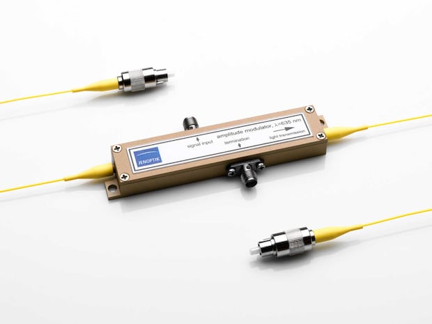
The integrated electro-optical amplitude modulator influences the amplitude of laser light very fast and with high dynamics.
The Jenoptik integrated optical amplitude modulator is a fiber-coupled electro-optical light modulator. It uses the Mach-Zehnder interferometer principle in waveguides, enabling you to transmit signals with particularly high modulation frequencies up to the gigahertz range. We offer modulators for wavelengths in the VIS and IR spectral range for this purpose.
With the standard version of the integrated optical amplitude modulators, the light is coupled in and out using polarization-maintaining single-mode fibers. You can also configure the light modulator with other fiber systems or connectors.
Benefits
- Powerful: High optical power stability and extinction ratios
- Fast: Broadband modulation into the gigahertz range
- Versatile: Can be used at a variety of wavelengths in the VIS and IR spectral range
- User-friendly: Couple in and couple out laser light easily via optical fibers and connectors
- Customized: Custom-made components for your requirements
Fields of Application
- Analog modulation with high dynamics
- Digital modulation
- Generate short pulses
- Shape pulses
- Exposure technology
- Laser scanning microscopy
- Pick pulses
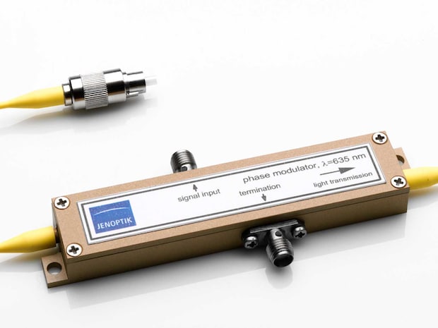
The Jenoptik integrated electro-optical phase modulator is a fiber-coupled electro-optical light modulator. You can use it in the VIS and IR spectral range.
With Jenoptik integrated optical phase modulators, you can influence the phase of light in particularly high modulation frequencies up to the gigahertz range. To do this, the modulator uses the rapid electro-optical effect of special crystals. You can also use the fiber-coupled light modulator in the VIS and IR spectral range.
In the standard version of the integrated optical phase modulators, the light is coupled in and out via polarization-maintaining single-mode fibers. You can also configure the light modulator with other fiber systems or connectors.
Benefits
- Powerful: High optical power stability
- Fast: Broadband modulation up to the gigahertz frequency range
- Versatile: Applicable in different wavelengths in the VIS and IR spec
- User-friendly: Laser light easily coupled in and out via optical fibers and connectors
- Customized: Customised components to meet your needs
Fields of Application
- Analog modulation with high dynamics
- Sideband generation
- Interferometric measurement technology
- Optical coherence tomography
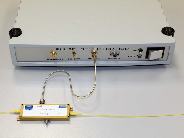
You can use the Pulse Selector IOM to control integrated optical amplitude modulators easily via the USB interface on your PC. The operating point of the light modulator is automatically stabilized in this process.
The Jenoptik Pulse Selector IOM is a control unit for integrated optical amplitude modulators. The pulse picker makes it possible to reduce the repetition rate of pulse lasers. Alternatively, you can use this control unit as a triggerable pulse generator.
The Pulse Selector IOM requires a TTL synchronous signal, which sets the laser repetition rate. You can control it easily using a command set via the USB interface on your computer. A photodiode is integrated into the pulse picker control unit. This enables you to use a feedback loop that automatically stabilizes the operating point of the amplitude modulator.
Benefits
- Versatile: Reduce the laser pulse repetition rate, or use it as a pulse generator
- User-friendly: Manual or automatic operation is possible
- Practical: Easy to use via the USB interface on your PC
- Feedback loop: Automatically control the stabilized operating point of the modulator
Fields of Application
- Reduce the laser pulse repetition rate in oscillator-amplifier systems
- Generate pulses
Product images


Optical Modulators: Technical information and instructions for use

Fig. 1.1: Scheme of an integrated-optical waveguide
1. Integrated-optical waveguides
Integrated-optical waveguides are able to guide light along a determined path analogue to optical fibre. They are fabricated on or in planar substrates and it is the properties of this substrate that determine the waveguide properties such as electrooptical modulation. The waveguide consists of a channel with higher refractive index compared to the surrounding material (Fig. 1.1).
The refractive index transition at the channel walls can be steplike or smoothly like described here. The light is guided by means of total internal reflection at the channel walls. Depending on the wavelength, substrate refractive index, refractive index increase, width and depth of the channel one or more transverse oscillation states (modes) can be excited. The single mode operation is of great interest since it is essential for the function of many integrated-optical elements.
Integrated-optical elements are usually provided with optical fibres particularly in optical communication technology. To achieve a good coupling efficiency to the fibre, single mode waveguides are typically three to nine microns in width and depth, depending on wavelength. Various elements like Y-branches, polarisers, phase- and amplitude modulators, switches or wavelength multiplexers can be implemented using integrated-optical waveguides.
2. The linear electrooptic effect
The linear electrooptic effect, also known as Pockels-Effect, is an optically second order nonlinear effect. It describes the change of the refractive index of an optical material if an external electric field is applied. The amount of change in refractive index is proportional to the electric field strength, its direction and the polarisation of the light. This interaction is described with the electrooptic tensor and is mostly anisotropic. The effect occurs in polar materials, including ferroelectric crystals. The preferred material for the fabrication of integrated-optical modulators is Lithium niobate (LiNbO3), which is also used for the modulators described here. In this crystal the strongest interaction occurs between the outer electric field in the crystallographic z-direction (E3) and z-polarised light with its refractive index n3. It amounts to:
$$\Delta n_3 = -\cfrac {1}{2} n^3_3 r_{33} E^3$$
The electrooptic coefficient r33 is 33 pm/V. The definite function requires the use of linear polarised light.
3. Polarisation of light and the modulators
Linear polarised light is required for definite modulator operation. Since waveguides in lithium niobate are polarizing, transmission losses are caused if the input polarisation is not linear or not sufficiently adjusted. At the input port a polarisation maintaining fibre is required.
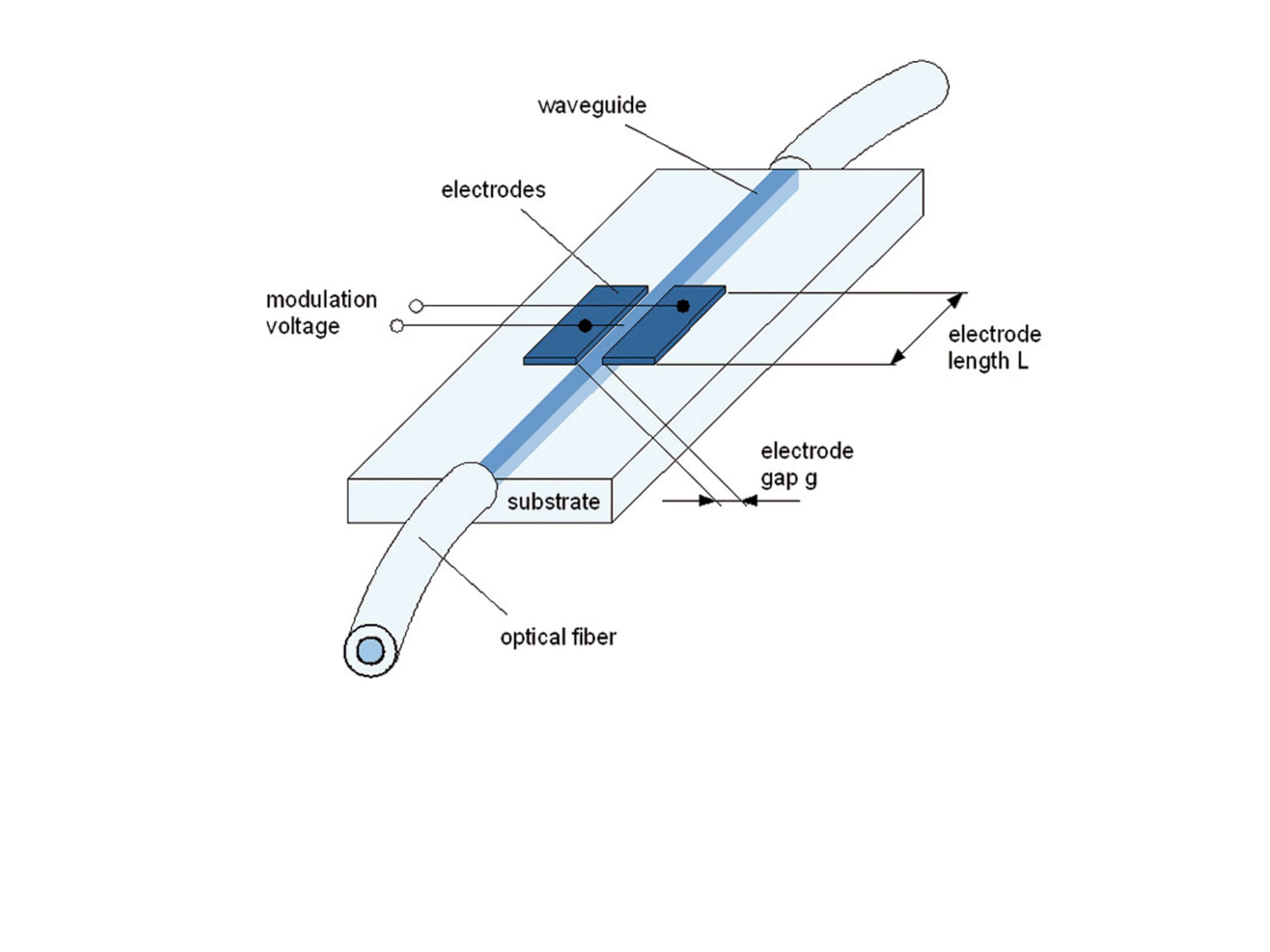
Fig. 2.1: Phase modulator
If an electric field is applied to a waveguide using electrodes of the length L, the refractive index changes in the area between the electrodes which is followed by a phase shift of the guided light. Because of the very small waveguide cross section it is not possible to place electrodes to produce a homogeneous electric field. Therefore a coplanar electrode arrangement on the crystal surface is preferred (Fig. 2.1). This generates an inhomogeneous field distribution with an efficiency G lower than 1. In lithium niobate modulators made in x-cut crystals it amounts to approximately 0,65.
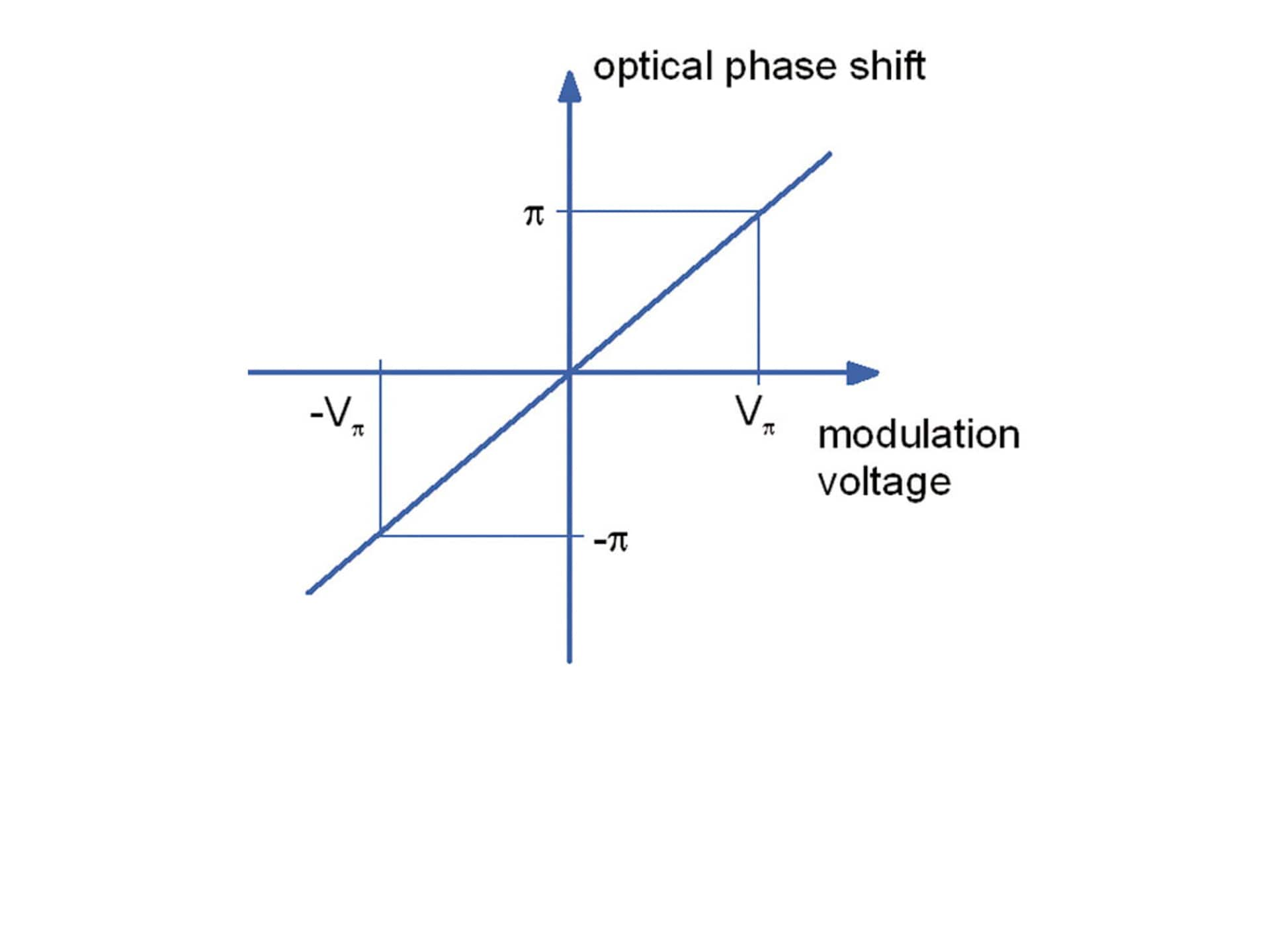
Fig. 2.2: Phase modulator characteristic curve
The phase shift is linear to the applied voltage (Fig. 2.2). A good approximation of phase shift can be described by:
$$\Delta \phi = \frac {\pi L}{\Lambda}n^3_3 r_{33}\cfrac {V}{g} \Gamma $$
The half of voltage Vπ, which causes a phase shift of π, is calculated by:
$$ V_{\pi} = -\frac {\Lambda g}{n^3_3 r_{33} L \Gamma} $$
This typically amounts to a few volts. For longer wavelengths it is higher than for shorter ones at a given electrode geometry. For example it can be expected to be 3 V in the red at 635 nm and 10 V in the telecommunication wavelength range about 1550 nm. Since the maximum applicable voltage is approximately ±30 V, phase shifts between 20 π in the red and 6 π at 1550 nm can be reached. Due to the very fast electrooptic response, together with low control voltages and the use of sophisticated travelling wave electrode geometry, it is possible to achieve modulation at frequencies in the gigahertz range.
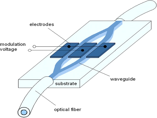
Fig. 3.1: Mach-Zehnder-amplitude modulator
A phase modulator is inserted into an integrated Mach-Zehnder interferometer to form an amplitude modulator (Fig. 3.1). It is advantageous to place electrodes in push-pull arrangement at both interferometer arms. Applying a voltage leads to a phase difference in both branches, which causes a change of the output power at the device output by means of interference. So the device transmission can be controlled between a minimum and a maximum value (Pmin to Pmax). A phase difference of π is needed for switching from on to off state or vice versa.
The needed voltage is called the half wave voltage Vπ of the amplitude modulator. Due to the push-pull-operation the half wave voltage of an amplitude modulator is the half of that of a phase modulator with equal electrode length. For example it can be expected to be 1.5 V in the red at 635 nm and 5 V in the telecommunication wavelength range about 1550 nm. The extinction ratio is given by the ratio of maximum to minimum output. It amounts typically to 500:1 in the red and more than 1000:1 in the infrared range.
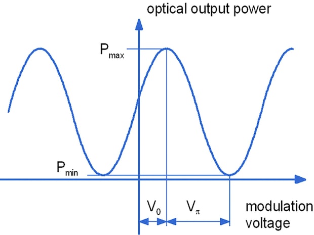
Fig. 3.2 Amplitude modulator characteristic curve
The output power versus control voltage is periodic (Fig. 3.2) in cosine form:
$$P = P_{min} + (P_{max} - P_{min})\biggl(\cfrac{1}{2} cos \biggl (\frac {\pi (V-V_0)}{V_\pi}\biggr) + \cfrac {1}{2}\biggr)$$
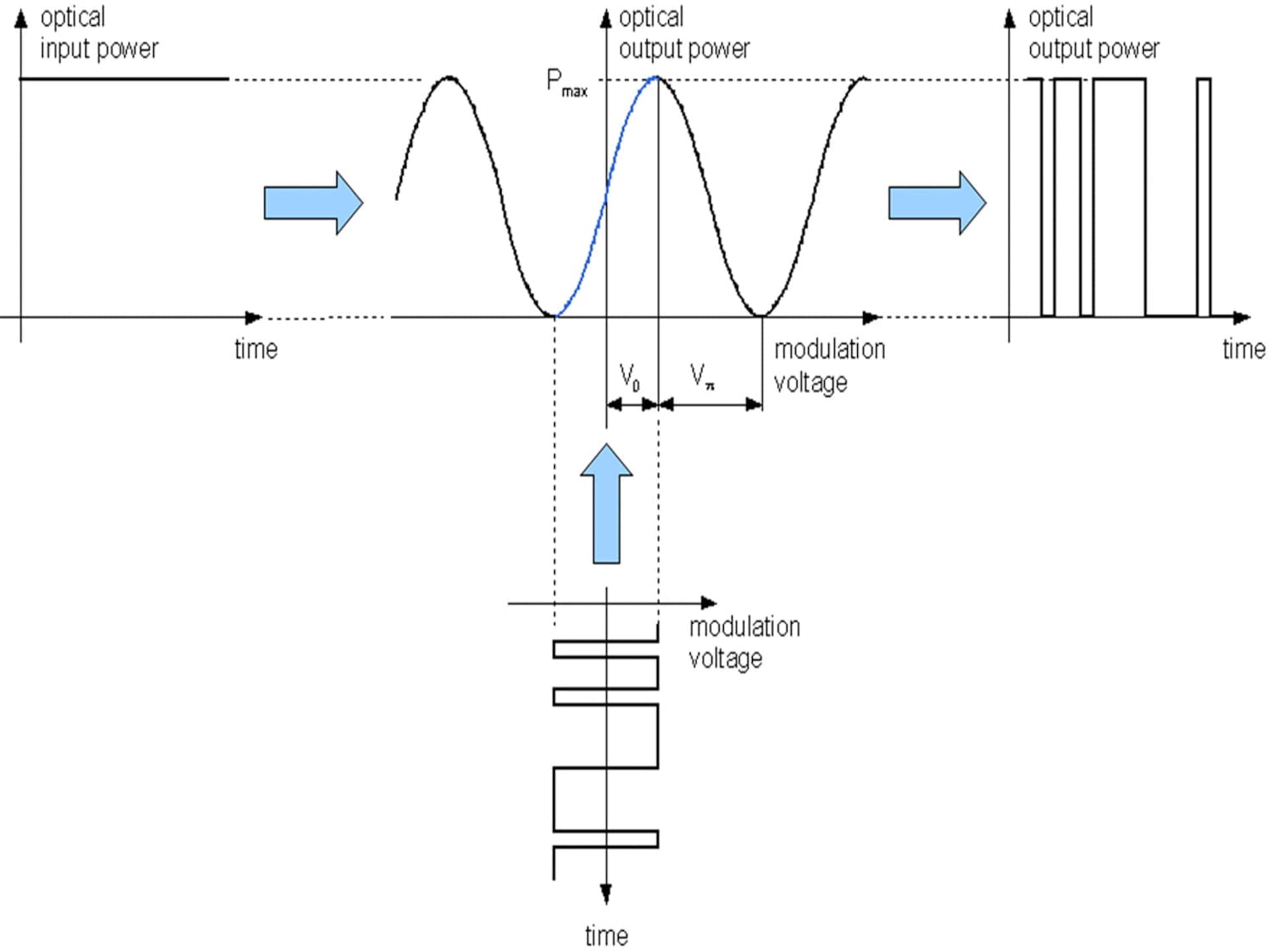
Fig. 3.3: Mach-Zehnder-amplitude modulator operation
The half wave voltage is required to switch from transmission state into the off-state and vice versa. Using a push-pull electrode arrangement it is the half of that of a phase modulator with identical electrode length. The operation point differs from the theoretical value V0=0. It must be controlled by special electronics.
Applying a rf signal as modulation voltage to the electrodes this electrical input is translated into an amplitude information (Fig. 3.3). This amplitude output depends on the voltage magnitude and shape, thus related to the position of the modulators operation point. The figure depicts the transmission of a binary pulsed electrical input into a binary optical output signal. If the voltage levels would not be correct, that is that the voltage is too high or the offset is not correct the modulator will react with non correct optical output levels in binary operation or with higher harmonics in analog operation.
Integrated-optical modulators for different applications and wavelengths are available in the substrate material LiNbO3. The selection is done depending upon the desired application.
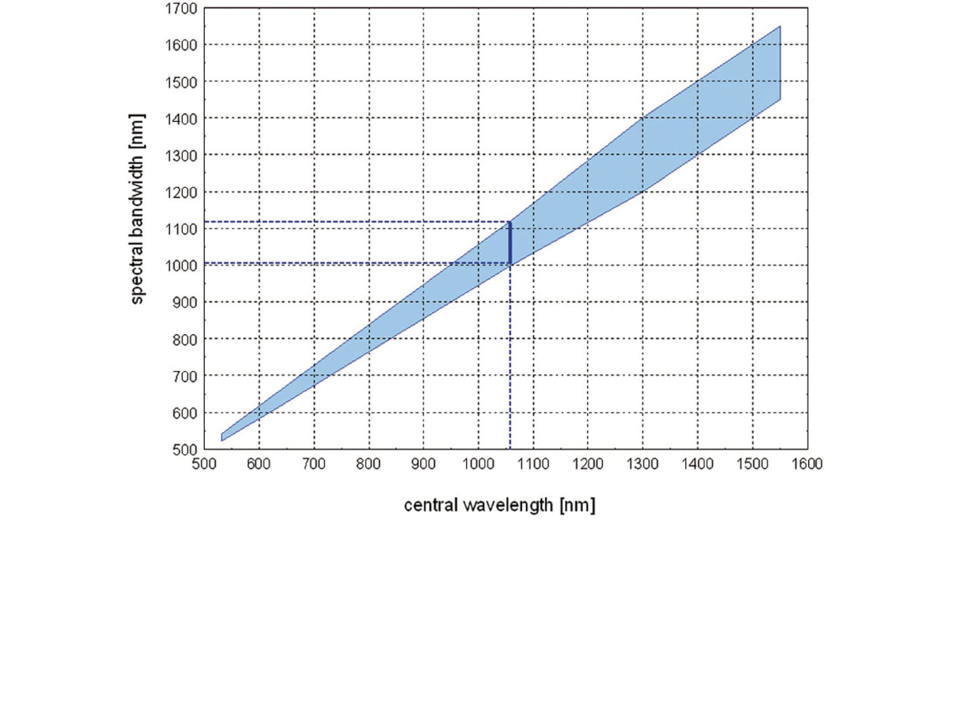
Fig. 4.1: Usable wavelength range
1. Wavelength and wavelength range
Various properties of the modulators, in particular the half wave voltage and insertion loss, depend on the operation wavelength. While the half wave voltage decreases at shorter wavelengths, the insertion loss increases, which is mostly due to Rayleigh scattering and a little due to absorption.
The usable wavelength range (spectral or optical bandwidth) of proper modulator operation is limited by the modal behaviour of the waveguide. It depends on the substrate material and the central wavelength. The singlemode operation and definite modulation is guaranteed within this range.
For a given central wavelength for which the modulator was fabricated the modulator can accept laser wavelengths out of a range which is coloured in the figure 4.1. For example at 1060 nm central wavelength the optical bandwidth is ± 40 nm, i.e. the modulator can operate between 1020 nm and 1200 nm. At longer wavelength the insertion loss increases due to waveguide cut-off and at shorter wavelengths the modulation is nondefinite due to interference of higher oscillation modes, respectively, leading to contrast loss in amplitude modulators or residual amplitude modulation in phase modulators. Amplitude modulation is possible with extinction ratio of more than 1000:1 in the near infrared spectral region, in the red the extinction amounts to more than 500:1
2. Technical data
The modulators are available for a variety of wavelengths (in the range from 635nm-1550nm, shorter wavelengths on request). In principle every wavelength can be provided if a laser whose wavelength is near to the desired wavelength is available. The modulator data of some standard wavelengths are depicted in the data sheets.
Linear polarised light is required for definite modulator operation. Since waveguides in lithium niobate are polarizing, transmission losses are caused if the input polarisation is not linear or not sufficiently adjusted.
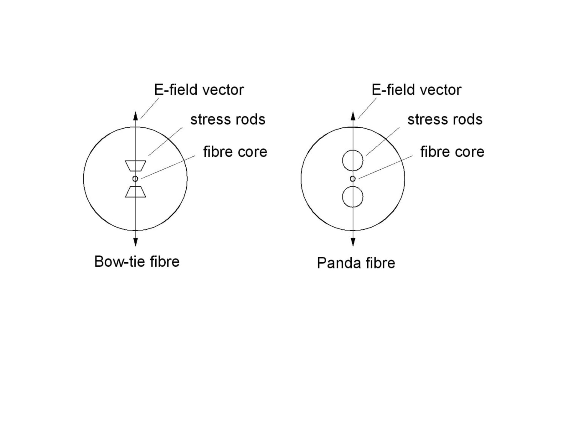
Fig. 5.1: Polarisation maintaining fibres in Bow-tie and Panda style
The modulators are produced with fibre pigtails with the standard length of 1 m. Other lengths are possible on request. At the input port a polarisation maintaining fibre is required. The output fibre is also polarisation maintaining, but standard singlemode (non-PM) fibres are available on request also.
The polarisation in the fibre is aligned to the stress rods in slow axis direction usually. Bow-tie fibres are used as standard. Panda fibres can be provided on request.
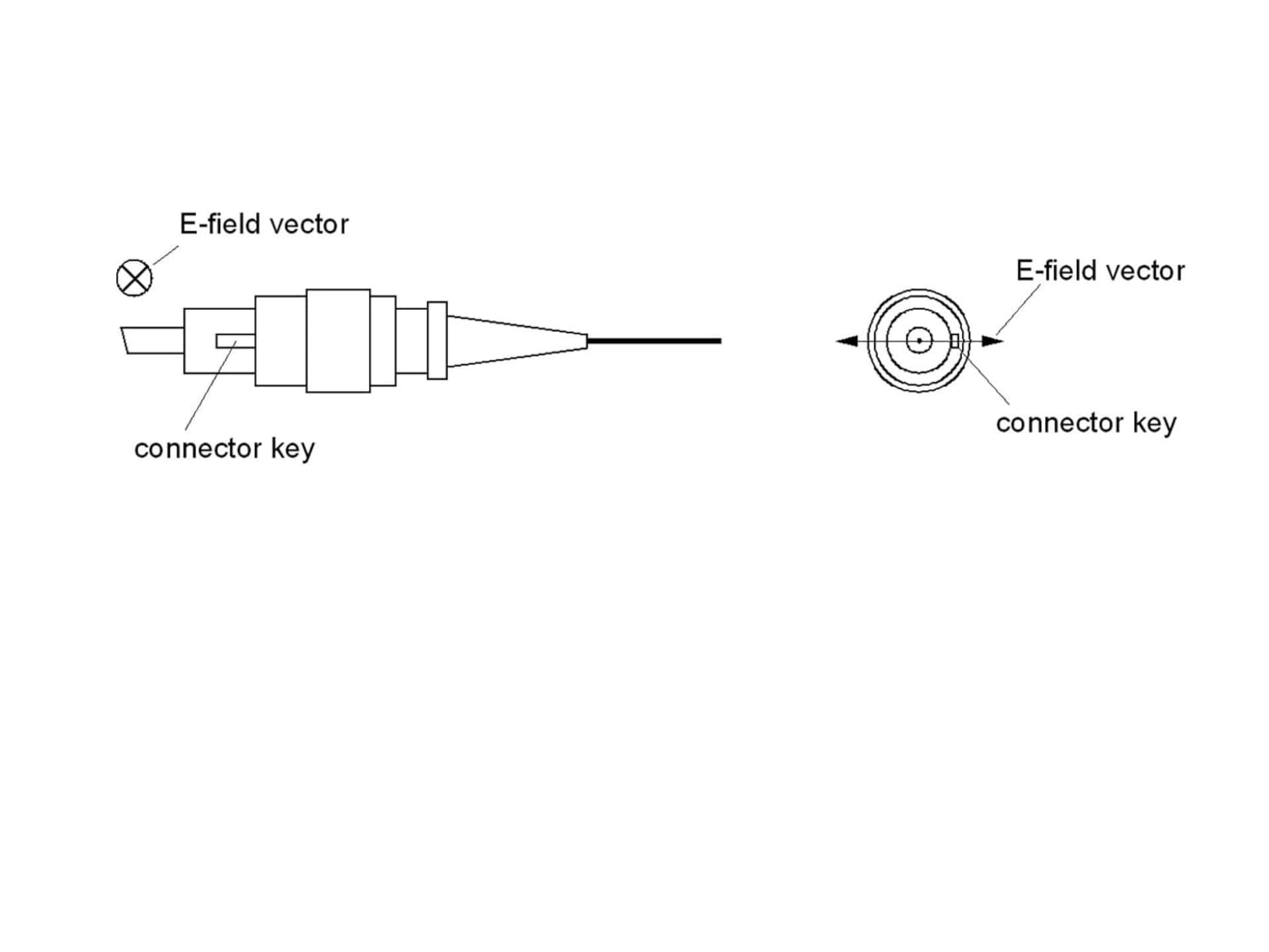
Fig. 5.2: Alignment of polarization in FC-connectors
The devices can be delivered with bare fibre ends or fibre connectors, preferably FC/PC- or FC/APC-connectors with 8° angled polished surface. The polarisation is aligned to the connector key as depicted in the figure 5.2. Other connectors or other polarisation alignment canbe provided on request.
The best connection between two fibres is the splice. It is very important to align the fibres best. Additional losses may occur if using fibre connectors because of the non-concentricity of the cores and the manufacturing tolerances of the connectors, especially for red light.
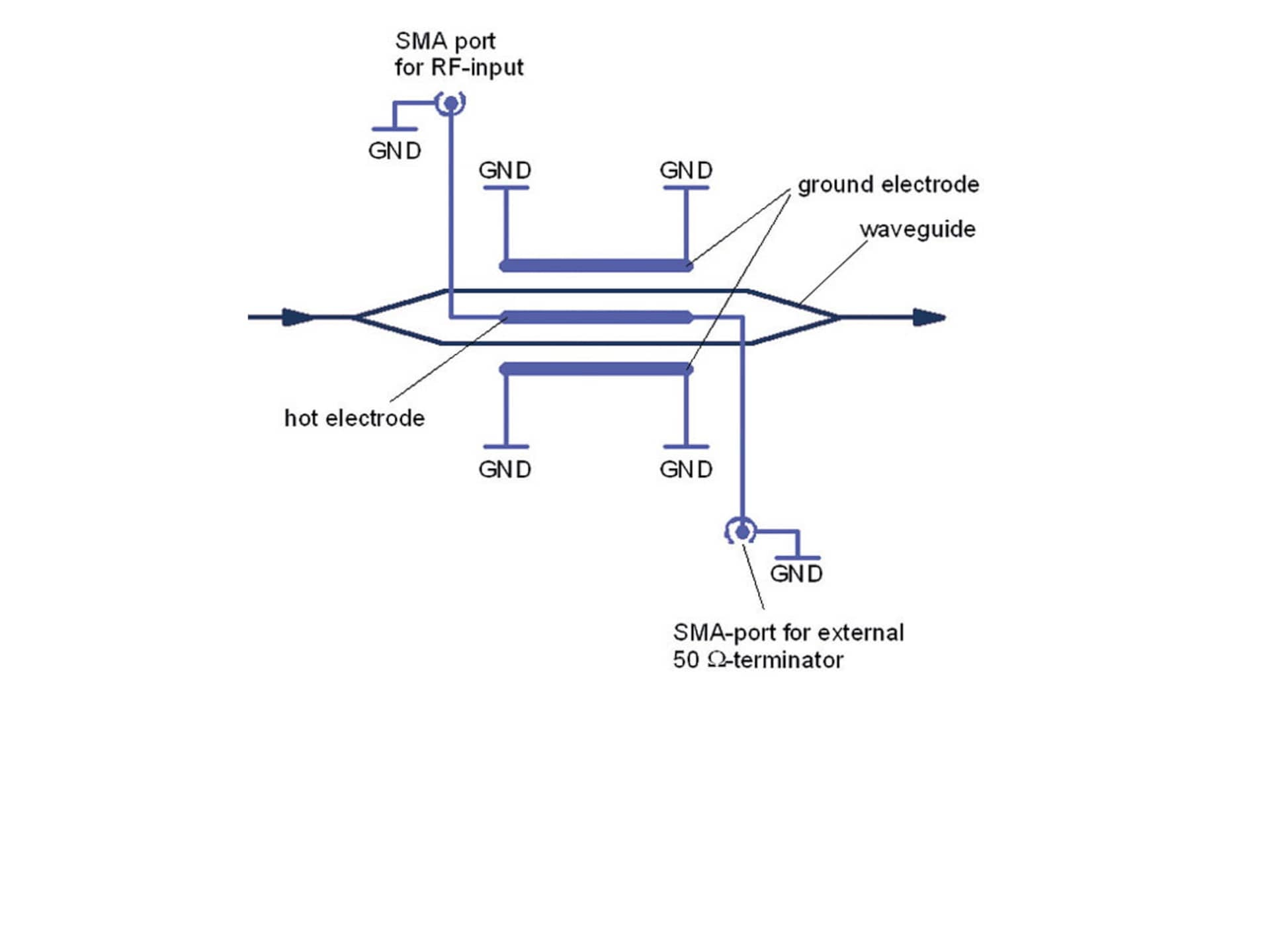
Fig. 6.1: Standard wiring scheme
1. Standard phase- and amplitude modulator wiring scheme
All phase modulators and the standard amplitude modulators are available without electronics inside the modulator case (Fig. 6.1). Both ends of the hot electrode on the modulator crystal are connected to SMA connectors. The ground electrodes are connected to the modulator case as well as the ground of the SMA connectors. One SMA connector can be used as rf-input, at the second connector a 50 Ω terminator is recommended to avoid reflections of the rf-signal which may disturb the modulation and the control electronics. The input modulator impedance is 50 Ω, the ohmic resistance between both ports between 5 and 10 Ω for the HF version and about 150 Ω for the standard version.The capacity amounts to app. 20 pF. The terminator can be removed for measuring purposes or to connect the modulator with further electronics. The modulator is electrically and optically symmetric. At higher modulation speed (500 MHz or more) the optical transmission direction must be the same as the electrical transmission direction.
The optical rise time is app. 200 ps for the HF version and 1 ns for the standard version if a short rise time electrical input signal is applied. A bias, which is necessary to control the operation point, causes a current through the hot electrode which may heat the electrode and the terminator. This can be prevented using a wiring scheme which is described in the further chapters.

Fig. 6.2: Wiring scheme with separated bias
2. Wiring scheme inside the amplitude modulator with separate rf- and bias-inputs
To separate the rf- and the bias-inputs a wiring scheme can be integrated into the modulator case (Fig. 6.2). All modulator electrodes are electrically isolated from the modulator case. The hot electrode is terminated internally, while the ground electrodes are connected to the ground by use of capacitors which cause a rf-connection, but a bias separation. So the bias can be fed by a second connector up to a frequency at which the capacitors become transmittant. This is approximately 10 kHz with 100 nF capacitors and approximately 100 kHz if 10 nF capacitors are used.
The optical rise time is app. 500 ps for the HF version and 1 ns for the standard version if a short rise time electrical input signal is applied. The bias does not cause a current through the hot electrode. The bias caused current is due to the capacitive resistance, thus frequency dependent. At dc the bias caused current is zero.
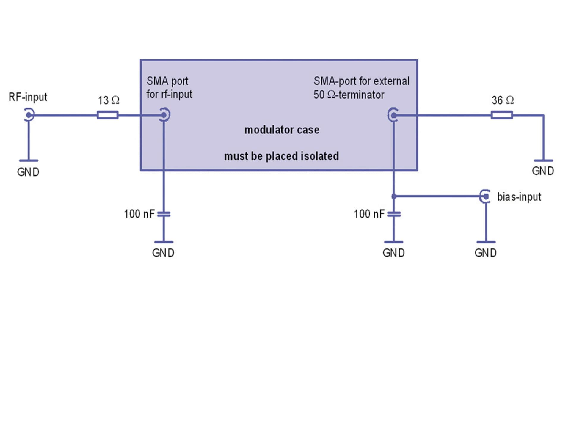
Fig. 6.3: External wiring scheme for bias separation
3. Separation of rf and bias using an amplitude modulator with standard modulator wiring scheme
The described bias scheme can be built up externally if a modulator with standard wiring scheme is used. Here the modulator case must be placed isolated and be connected to the ground using capacitors (Fig. 6.3). It is useful to place the modulator case and the surrounding circuitry in a rf-sealed case. If the lengths of the wires are short enough the electrical and optical properties are identical to the integrated version which was described in the previous chapter. The advantage is that the modulator can be removed from the outer case and be used as a standard one.
1. Driving of the modulator
For modulator driving no special driver is required. Any voltage supply with a controllable output voltage amplitude of 6-10 volts (connected to 50 W) depending on the modulator type, with a controllable offset and which is fast enough is suitable for modulator driving. If the supply output voltage is not sufficient an additional voltage amplifier may be necessary.
Adjustment of modulator operation
The modulator can be used for analog and digital modulation. Every voltage source can be used for modulator driving if its electrical output amounts to some volts connected to 50 Ohms and which is fast enough. The voltage which is applied to the modulator should not exceed 40 volts.
For analog modulation the periodical characteristic curve must be taken into account. For digital modulation a fast pulse generator can be used. Its upper and lower voltage level (i.e. amplitude and offset) must be adjustable independently. Then the modulator can be driven in two modes – the pulsed mode for short optical pulse generation and the switching mode for modulator switching.
The explanation will be done using a modulator with Vp= 2 V und V0= 1,5 V .
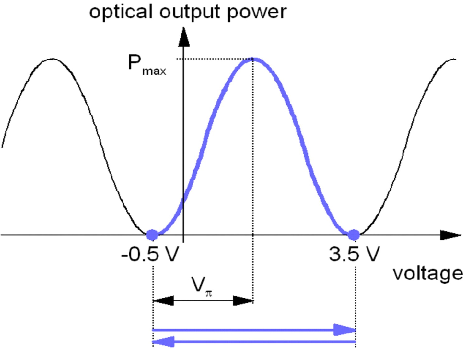
Fig. 7.1: Pulsed mode
The modulator is switched between two voltage levels for which the optical output power is zero (in the figure -0.5 and 3.5 volts). The modulator is switched from the off-state via the on-state to the next off-state (blue line and blue arrows in Fig. 7.1).
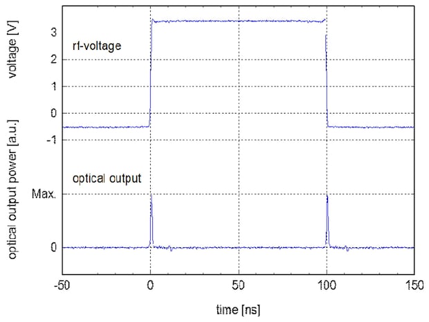
Fig. 7.2 Generation of 1ns pulses
It transmits a light pulse during the switching process. The optical pulse length corresponds to the rise time of the input voltage (1 ns in Fig. 7.2).
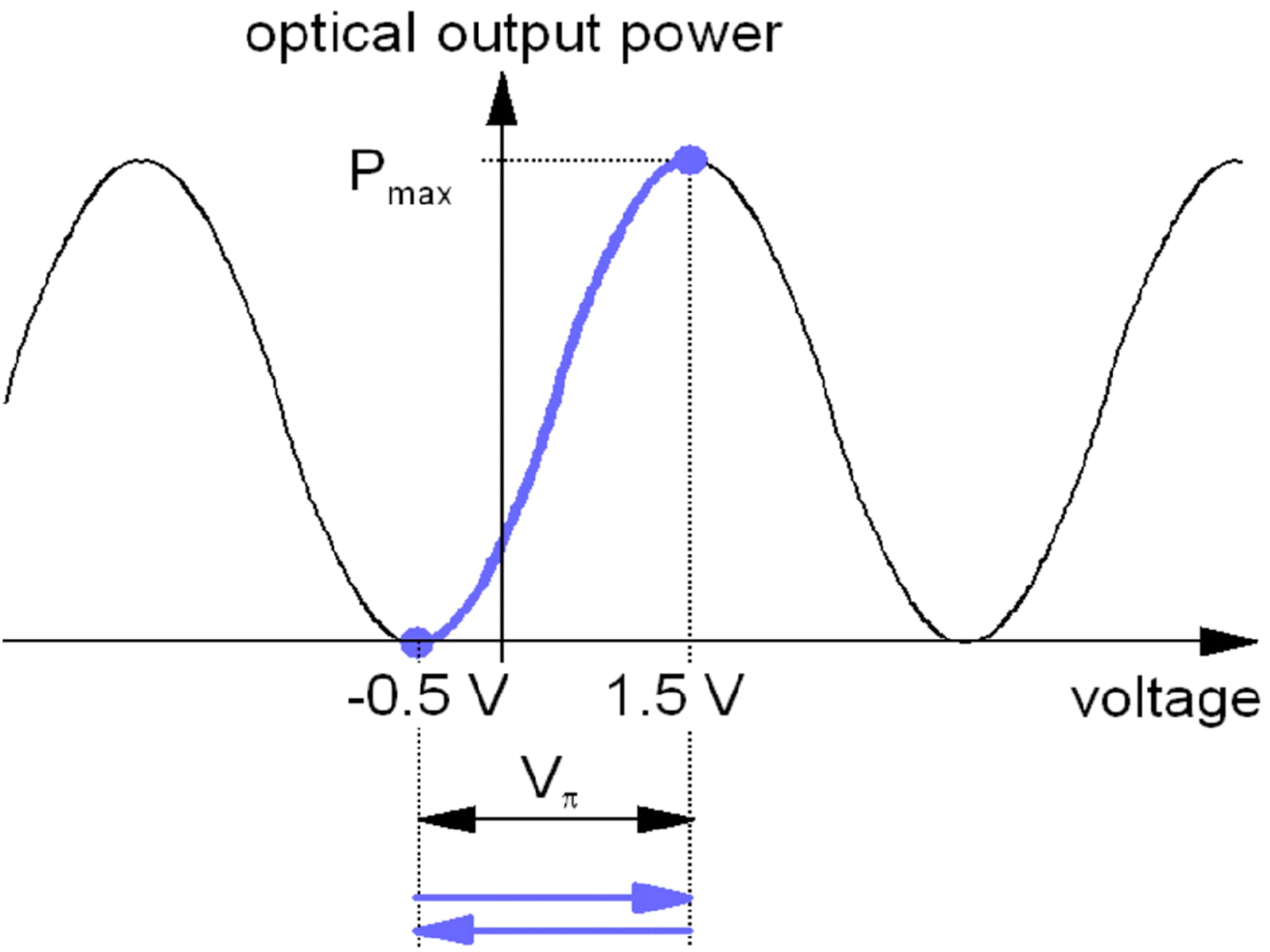
Fig. 7.3: Switching mode
Switching mode:
The modulator is switched between two voltage levels, for one the optical output is zero and for the other the optical output is maximum (in the figure -0.5 and 1.5 volts). The modulator is switched from the off-state to the next on-state (blue line and blue arrows in Fig. 7.3). It will be switched on or switched off vice versa. The optical rise time corresponds to the rise time of the input voltage.
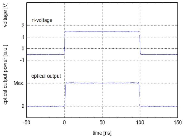
Fig. 7.4 Generation of 1 ns edges
If a light pulse should be generated its length corresponds to the time between on-switching and off-switching (100 ns in Fig. 7.4).
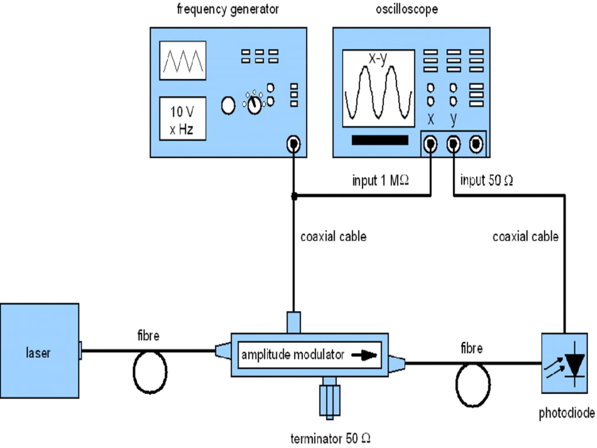
Fig. 7.5: Setup for operation curve measurement
2. Determination of V0 and Vπ
The parameters Determination of V0 and Vπ of the characteristic curve can be determined as follows:
A laser or laser diode is coupled to the modulator input fibre. The modulator output fibre sends its light into a photodiode. The electrical modulator input is connected to a frequency generator and a high ohmic oscilloscope x-input using coaxial cables. The photodiode is connected to the 50 Ohm oscilloscope y-input. The x-y- plot shows the characteristic curve, where Vπ and V0 can be determined. It is useful to save the curve data using a computer and to do a cosine fit then (Fig. 7.5).

Fig 7.6: Dc-drift: phase back-drift while dc-voltage is applied measured at an amplitude modulator
3. DC-behaviour of lithium niobate modulators
Waveguide modulators made of lithium niobate react on dc-voltage with the so-called dc-drift (Fig. 7.6). After applying a dc voltage a charge transport in the crystal takes place. That´s why the electric field which is applied to the electrodes is compensated partially, so that the effective electric field decreases partially with time. This process is related with the number of free charge carriers and with the dark- and photoconductivity of the crystal, respectively. Since the dark conductivity depends on the temperature and the crystal purity, while the photoconductivity depends on the crystal purity, wavelength and optical power density (i.e. the optical power in the waveguide), the duration of the compensation process depends on these values. It takes some minutes to some hours. The duration will become shorter the higher the temperature and optical power density and the shorter the wavelength. The compensation saturates at approx. 75 % of the initial value. The compensation time does not depend on the initial voltage. That means that the amount of the drift per time (i.e. the first derivate of the curve phase against time) becomes faster at higher dc voltages.
This partial compensation process of the electric field which passes the waveguide causes a partial back-drift of the initial optical phase shift which was caused by the applied voltage. At phase modulators it can be measured directly by use of an interferometer. In the case of amplitude modulators the optical phase shift is followed by an amplitude modulation of the optical output due to its cosine characteristic curve. This can be measured as shift of V0. Vπ does not change its value.
The diagram shows an example of the phase drift which was measured at a 1550 nm amplitude modulator with an optical power of some milliwatts at room temperature. The phase is given in % of the initial value and was calculated by use of the cosine characteristic curve of the modulator. The applied voltage (2V) was a little higher than Vπ (1.59 V), that means that the inital phase has been 1,25 π. It is to be seen that the time which is needed for stabilisation is more than one hour if the modulator is used in the infrared at moderate optical power. The drift will be faster if higher optical power or shorter wavelengths are used, but the modulator reacts more on changes of the light and environmental conditions also.
A stabilisation of the operation point can be done as follows:
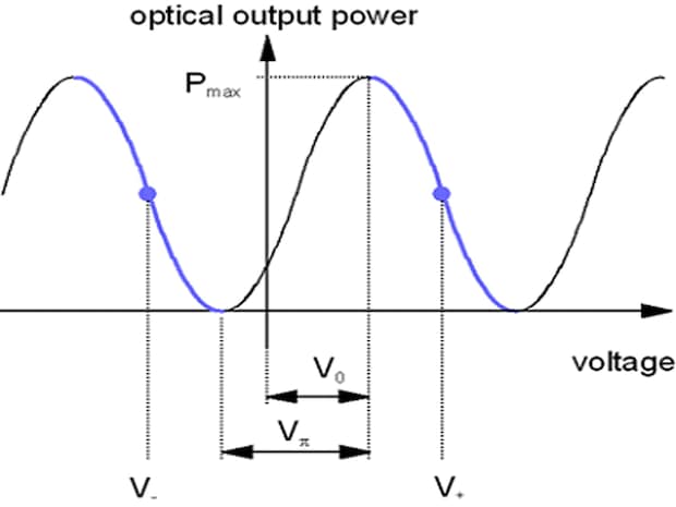
Fig 7.7: Modulator characteristic curve with two equivalent operation points
3.1. Dynamic mode:
Due to the periodicity of the output signal it is possible to modulate at different parts of the characteristic curve, which are differing by a multiple of 2*Vπ . The operation point should jump between two equivalent voltage values with alternating sign, in the sketch (Fig. 7.7) depicted as V- and V+ . Then the modulation occurs alternating on both red parts of the characteristic.
To avoid dc-drift the applied voltage V should be measured and integrated for a time which is short enough against the duration of the dc-drift (< 1 second) while the modulator operates at the operation point V- . The value A- with: $$A_- = \int_{V_-} V (t) dt $$
After this the operation point has to switch to V+ where the modulator operates until the value A+ with $$A_+ = \int_{V_+} V (t) dt $$ is reached, where $$ |A_+| = |A_-| $$ must be fulfilled.
Then the operation point has to switch to V- again and so on. This causes that the average value of the applied voltage is zero and no dc-drift can occur. It must be taken into account that the modulator passes the periodic characteristic while changing between V- and V+ which produces an unwanted optical power modulation.
3.2 Bias mode
The operation point must be set using a bias. The bias can be applied using a bias-T in front of the rf-input of the modulator, which adds a dc or low frequency bias to the rf-signal. But this causes an electrical current through the modulator electrodes and the terminator which is a load for the voltage source and causes a heating of the electrodes and the terminator. The better way is to use an external bias scheme or an integrated bias circuit like depicted in the previous chapter. But the bias mode cannot avoid the dc-drift.
If the modulation is periodic, that means the integrated applied voltage is constant and the temperature as well the optical power will not be changed, the drift will saturate after a certain time and a stable operation regime can be reached by correcting the bias voltage.
In the case of nonperiodic modulation or changing environmental conditions a feed back loop must be used. A part of the optical modulator output must be split up using a fibre coupler or a partial mirror and fed into a photodiode. The type of the correction electronics depends on the modulation. No recipe can be given here which fulfils all thinkable demands. For example if short optical pulses with relative long delays have to be generated or pulses have to be picked it is sufficient to hold the bias on the voltage which causes a minimum average output power since the integrated underground signal is a considerable larger part of the average power than the pulse power itself. If an analogue modulation is necessary the actual output signal must be measured and be compared with the desired output signal. In some cases, for example in image generation, it tis possible to measure the characteristic curve automatically in a time where the modulator output is not needed. The amount of the bias voltage should not be too large since the slope of the phase shift curve becomes steeper at higher biases and the correction must be done in shorter times.
We specify the minimum optical rise time (200 ps) as optical reaction on a binary input signal. This corresponds to app. 1 Gbit/s and 500 Gbit/s, respectively. The reason for this limitation is that the half wave voltage is almost constant up to app. 1 GHz sine. Then it rises up to approximately the triple of the low-frequency one at 6 GHz sine. Because of the higher harmonics of the square-wave input the rise/fall time is limited to app. 200 ps. Pure sine modulation is possible up to app. 6 Ghz, but with higher Vπ.
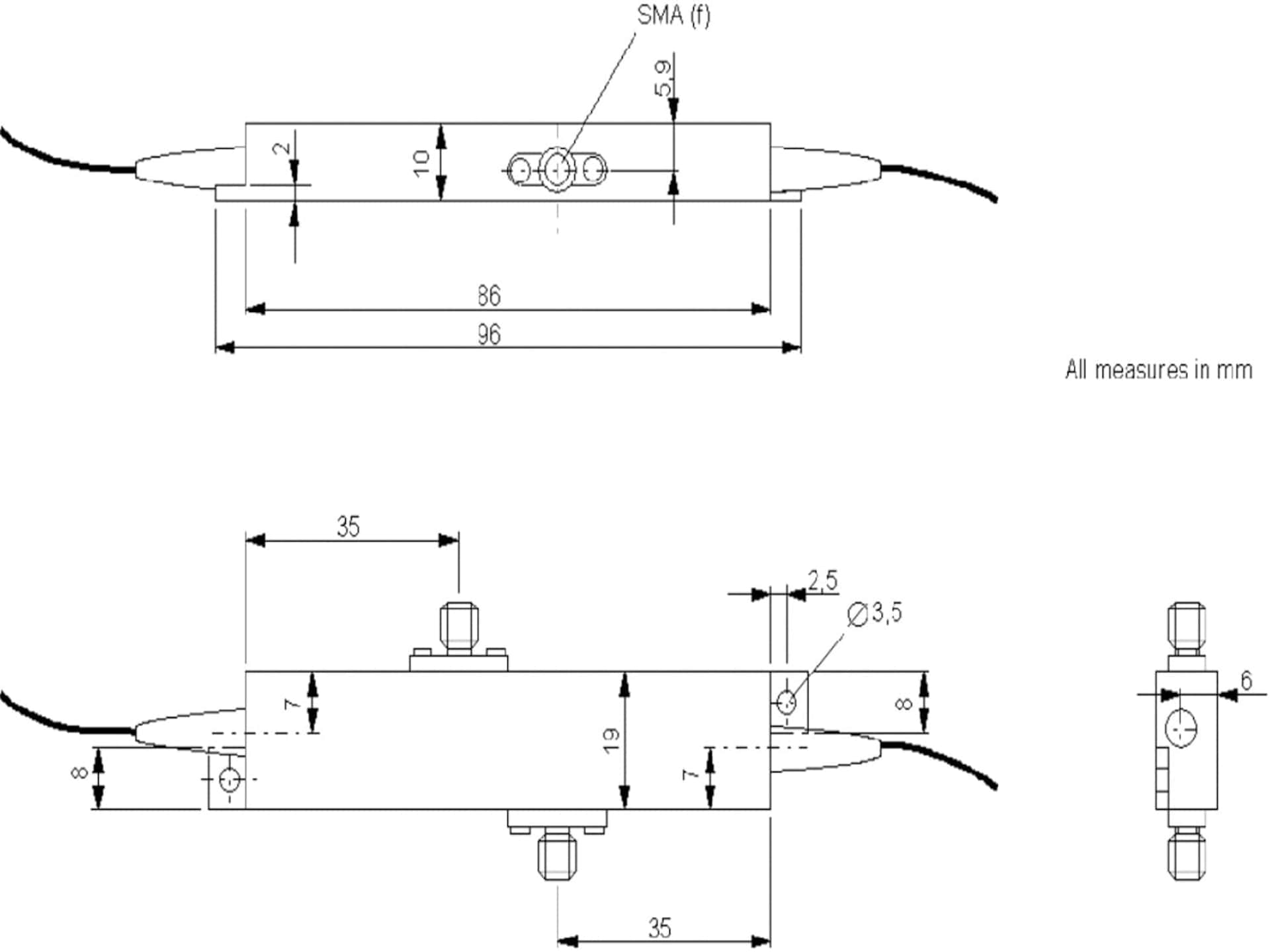
Fig. 8.1: Standard phase and amplitude modulator case
1. Size AMxxx
The modulators are available in standard cases. Their measures are sketched as follows:
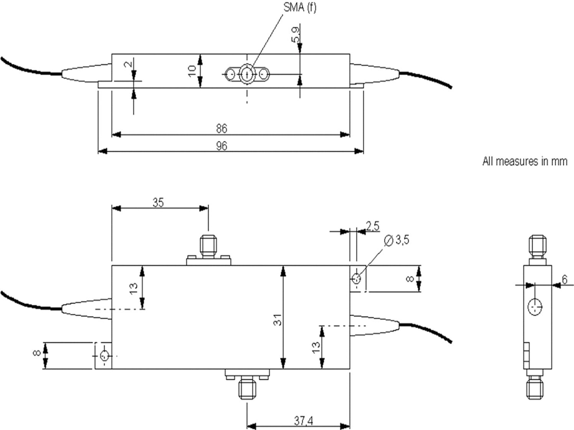
Fig. 8.2: Widened amplitude modulator case with separated bias input
2. Size AMxxxb
Their measures are sketched as follows:

Fig. 9.1: Generation of a 1 ns pulse
1. Pulse slicing
One essential modulator application is to generate and to shape short pulses using cw laser light. The advantage is that the pulse shape can be controlled independently on the laser type. This is needed in some laser applications, especially in fibre oscillator-amplifier arrangements. For example a short light pulse is generated if an electrical egde with the amplitude 2xVπ or an electrical pulse of the amplitude Vπ is applied (Fig. 9.1 and 9.2). An analogue temporal shaping of light pulses can be done in similar manner, like it is depicted using a two-step pulse (Fig. 9.3).
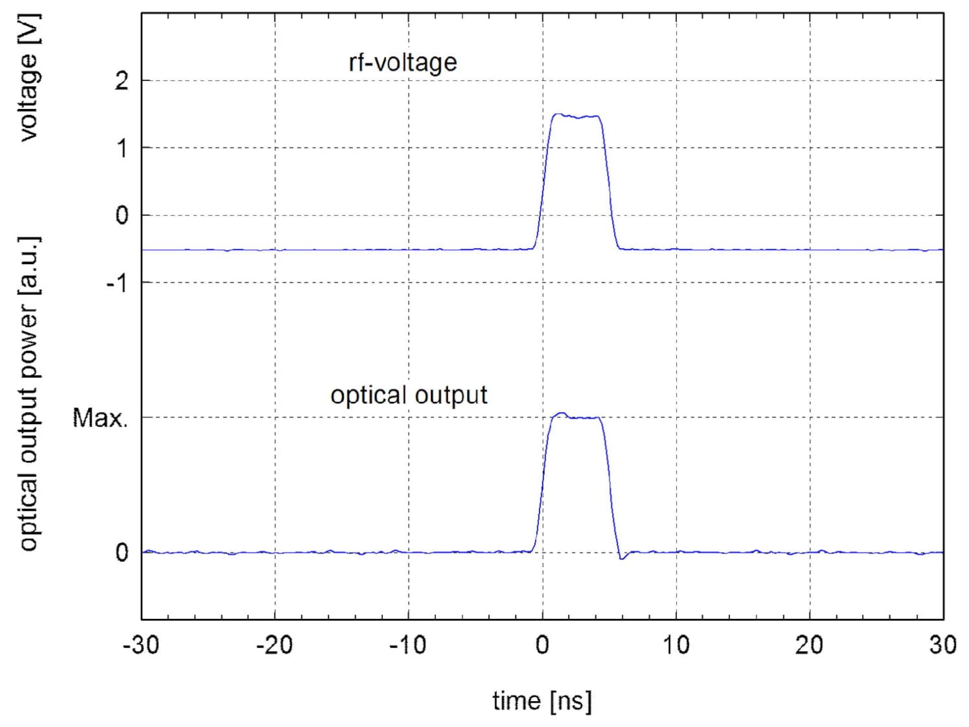
Fig. 9.2: Generation of a 5 ns pulse
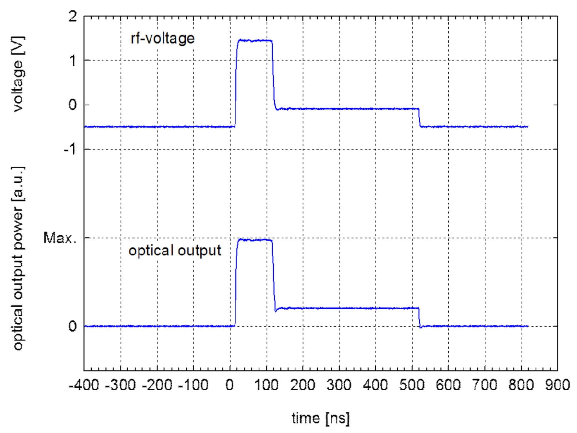
Fig. 9.3: Generation of a two-step pulse
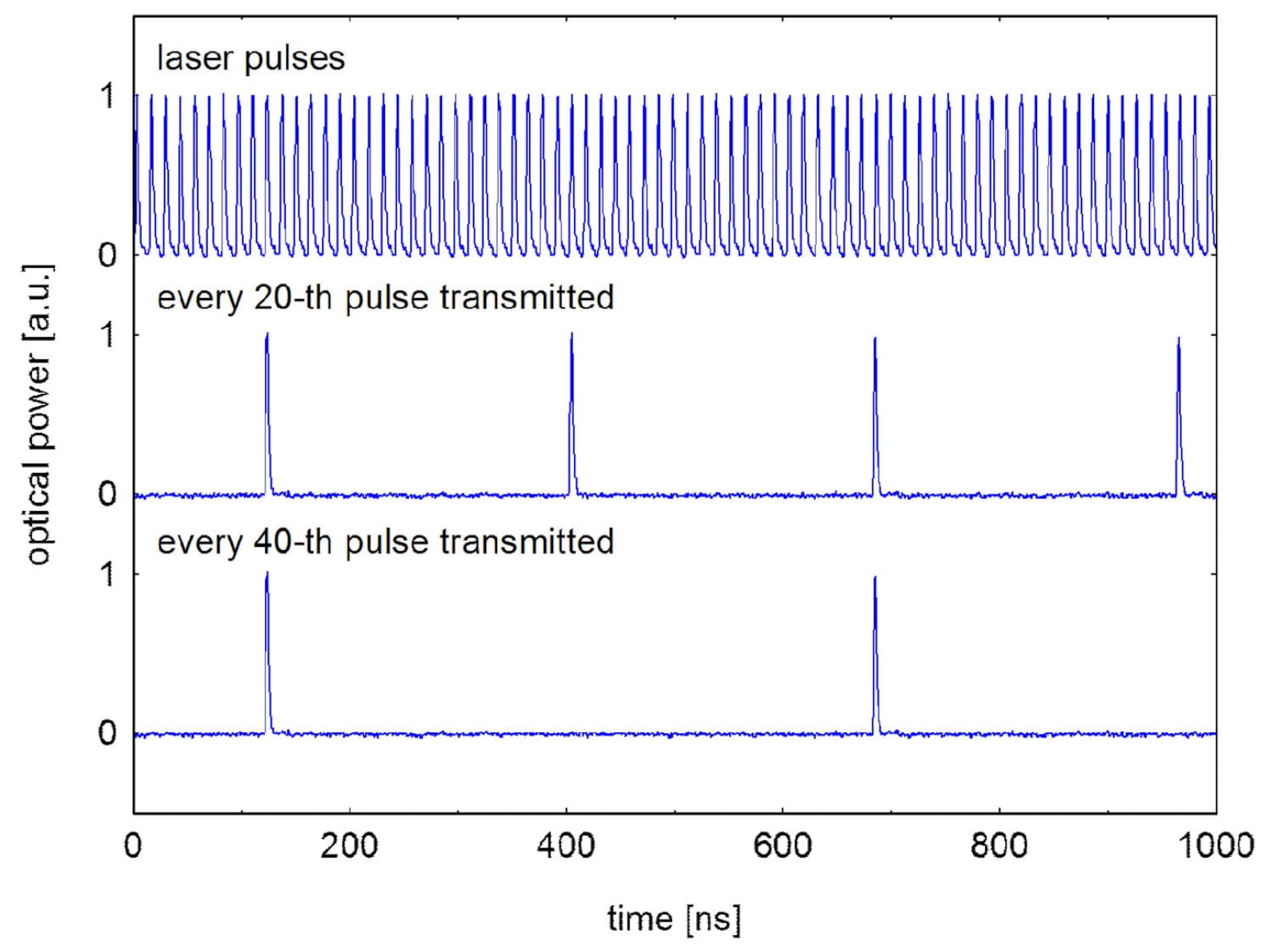
Fig. 9.4: Pulse picking
2. Pulse picking
Single pulses or pulse combs can be selected from fast laser pulse chains. Thus the amplitude modulator operates as pulse picker to reduce the repetition rate of the laser. The following example shows the pulse picking from a 1060 nm, 150 fs, 76 MHz pulse chain with picking factors 20 and 40, respectively. In most cases picking by a factor between 100 and 1000 is necessary.
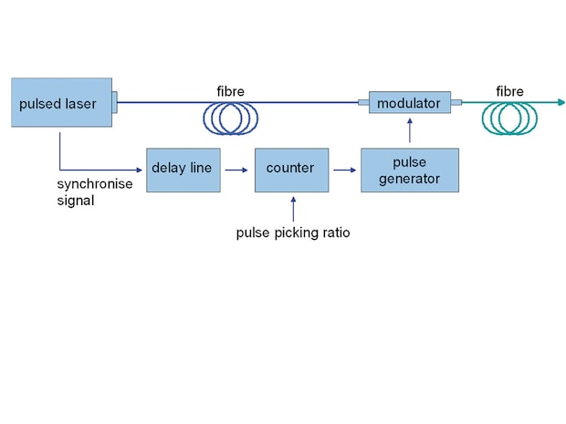
Fig. 9.5: Driving scheme of the pulse picker
The operation principle acts as follows (Fig. 9.5):
A synchronise signal which is taken from the pulsed laser feeds an electrical delay line. This is used to equalise the runtimes of the pulses in the fibre and wires and the driver operation time. A counter counts the synchronise signal pulses up to a preset number. The counter output pulse feeds a pulse generator which drives the modulator thus opening it for the transmission on one or a number of light pulses.
Description of terms
Insertion loss (D)
- Loss of optical power if light is transmitted through the modulator
- D=10 lg (Pin/Pout)
- Pin: optical power which is guided in the input fibre
- Pout: optical power which is guided in the output fibre if modulator transmission is maximum (on-state)
- Measurement using fibre cut back method
Extinction (E) (contrast ratio)
- In the case of amplitude modulator the ratio of transmitted optical power in on- and off-states
- E=Pmax/Pmin
- Measurement at dc-voltage
Half wave voltage (Vπ)
- In the case of amplitude modulator the voltage difference for switching the modulator from on- to off-state or vice versa
- In the case of phase modulator the voltage difference for shifting the phase of the optical output signal by π
- Measurement frequency 1 kHz
Offset (V0)
- Lowest voltage compared to 0 V, at which the transmission of an amplitude modulator is maximum (on-state)
- Measurement frequency 1 kHz
Polarisation of output fibre
- Polarisation ratio of the light in the output fibre if a polarisation maintaining fibre is used
Spectral bandwidth
- Possible deviation of the operation wavelength from the central wavelength of the modulator without substantial diminution of extinction and insertion loss (increase of insertion loss ordecrease of extinction by 10% with respect to the central wavelength)
Upper critical frequency
- Frequency at which the effect of the electrical input on the optical output signal decreases by one half
Optical rise time
- Time in which the optical signal of an amplitude modulator rises or falls between the 10% and 90% values of maximal transmission if an electrical step-function is applied to switch the modulator between on- and off-states
Thema: Wellenleitermodulatoren für neue Einsatzgebiete
Veröffentlichung in Fachzeitschrift: Optik & Photonik 1/2010Amplitude Modulator
Phase Modulator