Shaping the digital future: high-precision optics and micro-optics for high-volume data communication
Solutions for a wide range of applications: from fiber optics to free space communication
With our expertise in micro-optics and optics, we provide tailored solutions for optical transceivers, fiber optic communications, free space communication and other applications, helping to shape the future of data transmission.

Jenoptik optical and microoptical solutions for optical data communication applications


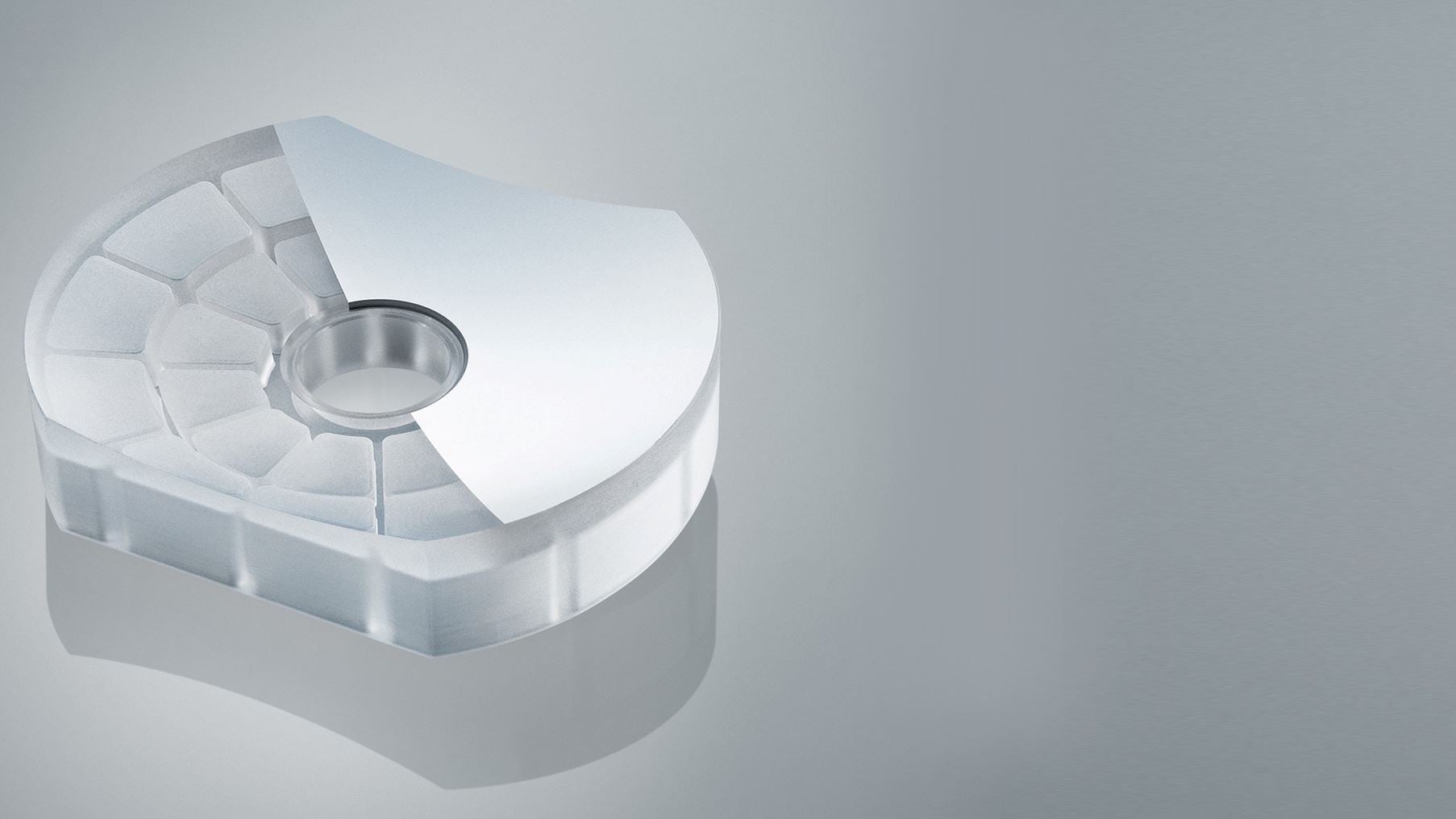
Microoptics for fiber coupling in optical transceivers and co-packages optics
Enhance optical performance
With cutting-edge microlens arrays no larger than millimeters, designed to boost light coupling efficiency and spatial resolution for precise fiber coupling.
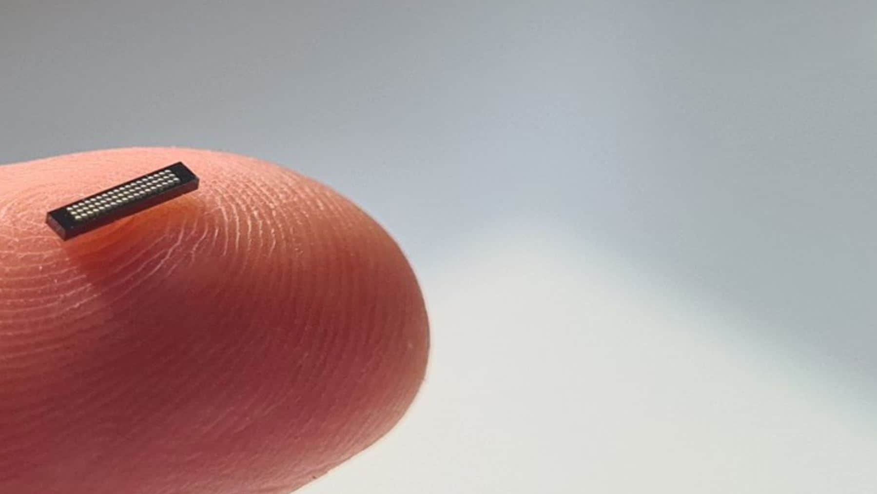
Testing of Photonic integrated circuits (PICs), the heart of next-generation transceivers/pluggables
Thanks to photonic integrated circuits (PICs), integrated photonics is becoming the key to fast and growing data communication. The advantages are higher speeds and bandwidths, lower energy losses, reduced sensitivity to interference, and a higher degree of miniaturization and integration.
Testing PICs is a critical step in the development and manufacture of photonic systems to ensure that the PICs meet the required specifications and performance characteristics. This is especially true for the mass production of high-performance PICs for next-generation transceivers, which form the backbone of the data center network.
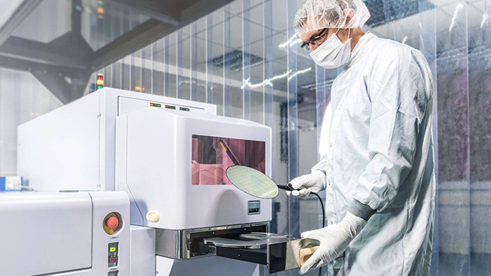
The increasing complexity of chips and the goal of reducing costs through economies of scale are driving demand for fast, automated, and parallelized wafer-level testing. To ensure that these tests are reliable and reproducible, they must be standardized and performed in a uniform test environment. This is the only way to achieve the high yields and low scrap rates required by modern silicon photonics fabs.
Test PICs at wafer- or die-level
Verify known-good dies (KGDs) before packaging to remove defective PICs from the process at an early stage. Qualify photonic integrated circuits (PICs) more efficiently by testing optical and electrical functionalities simultaneously at the wafer-level.
Customized hybrid probe cards for your PIC tests

In the fast‑growing silicon‑photonics market, wafer‑level testing must deliver high‑precision optical and electrical measurements in a single, high‑throughput test station. Conventional approaches that use separate optical and electrical probe cards create cumbersome hand‑offs, long set‑up times and a higher risk of mis‑alignments.
UFO Probe™ Technology turns this challenge into a solution with hybrid optical/e‑electrical probe cards.
- One‑board design – a compact PCB that houses both an optical test module and an electrical test module on the same card.
- Single-card design – a compact design that monolithically houses both an optical test module and an electrical test module on the same card.
- Seamless integration – IC standards as a blue-print making the system ready to use immediately.
- Proven needle technology – the electrical side relies on established needle probes from leading manufacturers, while the optical components are supplied by Jenoptik, the expert in optics and photonics.
- High throughput, minimal set‑up – the integrated concept eliminates hand‑offs and alignment errors, enabling fast, reliable measurements in production
Qualify photonic integrated circuits (PICs) more efficiently by testing optical and electrical functionalities simultaneously at the wafer level.
High-precision optics for the use in Space
Need for Speed and Reliability
- High-Speed Internet everywhere on earth
- Point-to-point-communication from continent to continent
- Quantum Cryptography – 100 % secure connections

Requirements and conditions for products in Space (LEO and GEO)
To be successful in Space, products must meet specific requirements and withstand harsh conditions:Thermal conditions: Temperatures in Satellites range from -100°C to +60°C. Optical assemblies must withstand this temperature range without losing performance.
Shock and vibration: Products must withstand the shock and vibration during launch of a spacecraft. This includes suitable bonding surfaces and materials, such as glass, that ensure optical components and systems arrive functional in orbit and maintain their optical precision and performance.
Radiation intensity: Radiation in LEO is extremely high and consists of various types, including ionizing and X-ray radiation. Components must be made of radiation-resistant materials to withstand this radiation. For example, the coating must not deteriorate.
Explore the edge of space
Discover how cutting-edge optics like lightweighted mirror systems or optomechanical subassemblies for beam splitting - both operating in telescopes used in space - are pushing the boundaries of free space optical communication. Withstanding extreme temperatures, intense radiation, and intense vibrations, our optics enable faster, more reliable data transmission. exploration and communication.