RecommendMail Facebook LinkedIn
Groundbreaking ceremony for the new high-tech fab in Dresden
Jenoptik is investing more than 70 million euros in new and state-of-the-art production facility for micro-optics and sensors.
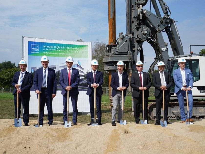
Construction work on the Jenoptik Group’s new high-tech fab at Dresden Airport Park began today, September 6, 2022, with a groundbreaking ceremony attended by Saxony’s Minister-President Michael Kretschmer and Mayor Stephan Kühn, Dresden’s Councillor for Urban Development, Construction, Transport and Real Estate. The two politicians ceremonially broke ground together with Jenoptik Executive Board members Stefan Traeger and Hans-Dieter Schumacher and other representatives of the photonics group. In the afternoon, the company invites its 60 employees at the site together with their families to a summer party on the construction site.
"Dresden will become a main location for our micro-optics activities. We deliberately chose one of the most important locations for the semiconductor industry in Germany and Europe, where many global companies and research institutions of the industry are present," said Stefan Traeger, President & CEO of JENOPTIK AG.
Minister-President Michael Kretschmer: "The construction of Jenoptik’s new cleanroom factory in Dresden is a strong signal and makes an important contribution to the technological advancement of microchip manufacturing. The settlement of Jenoptik proves once again the attraction of Silicon Saxony and shows how important an existing good local network is to attract new companies to the location. I am pleased that Jenoptik is convinced of this semiconductor ecosystem, which is unique in Europe, and I am sure that all partners at the location will benefit from this settlement."
"The federal state capital Dresden is proud to have been able to accompany such an innovative and globally active East-German group in its growth for years now. The new Jenoptik fab shows that Dresden offers an ecosystem with excellent research facilities, highly qualified specialists and strong partners in which high-tech companies are constantly developing," said Dresden Lord Mayor Dirk Hilbert about the Jenoptik investment.
Extremely demanding construction and manufacturing environment
Jenoptik is investing more than 70 million euros in the new high-tech fab with a total of 11,000 square meters of net floor space, including 2,000 square meters for clean room production. Production is scheduled to start at the beginning of 2025. The new high-tech fab will manufacture micro-optics and sensors, which are mainly used in semiconductor lithography systems. Production will take place in clean room classes ISO 5 and 3, which also meet the highest requirements for vibration-free production and temperature stability. Comprehensive vibration monitoring is also in place during the construction of the fab in order to not disrupt the production processes of neighboring companies in the industrial park.
High environmental standards taken into account
In addition to precise manufacturing conditions, the high-tech fab also meets high environmental standards: Jenoptik aims to meet the "KfW 40 Standard" and "LEED Gold Standard Certification", currently the most comprehensive and stringent building criteria in terms of sustainability. To achieve this, comprehensive environmentally friendly measures are planned, such as a photovoltaic system, recycled materials during construction, a highly efficient building envelope including greening, cold and heat recovery, and intelligent control technology.
Photonics as a growth driver
Jenoptik has been active in Dresden since 2007 and currently has more than 60 employees on site. With the new production facility, Jenoptik will concentrate manufacturing in Dresden, which is currently spread across several smaller external locations. The photonics group is creating 60 additional high-quality jobs and increasing its local workforce to a total of well over 120 employees. In addition to Dresden, Jenoptik also manufactures its high-precision and micro-optics at the Thuringian sites Jena and Triptis (polymer optics), in Heerbrugg, Switzerland, as well as in Jupiter (Florida) and Huntsville (Alabama), USA. In the Advanced Photonic Solutions division, around 2,300 employees work on photonic technologies for the success of future industries.
Optics & sensors for the semiconductor equipment industry as well as other sectors such as medical technology & life sciences or IT infrastructure & communications are key growth drivers for Jenoptik. As a photonics group, Jenoptik is focusing on expanding these business areas, which are expected to generate around 75 percent of the 1.2 billion euros in revenue targeted by 2025. "To this end, we are investing both in the acquisition of companies, as demonstrated by our recent acquisitions, and in organic growth, for example by expanding our own infrastructure. The Dresden high-tech fab is the largest single investment in Jenoptik’s recent history," said CFO Hans-Dieter Schumacher.
With the new fab, Jenoptik is meeting the rapidly growing demand for photonic solutions. Industry experts predict further growth for the semiconductor equipment industry – the main customer of the new fab’s products – in the next years.
Focus on high demand for micro-optics
An important area of application for micro-optics is the semiconductor equipment industry. For example, micro-optical sensors enable the exact positioning of wafers during lithographic processes for chip production. Applications include both DUV and EUV lithography. Micro-optics and micro-optical sensors are characterized by highest precision in smallest space and very flat design. They direct light by means of micro- and nanostructures and – unlike classical optics – are manufactured in a lithography process similar to semiconductor production. In addition to chip production, they are used in other primarily technological manufacturing processes that require highly precise and or very flexible positioning of light for process steps, for example in laser material processing, or quality assurance, for example in inspection processes. The very light and small individual components, often only a few micrometers in size, can be combined to form miniaturized scanning and switching systems with flexible multiple applications.
Fab on the web: www.jenoptik.com/hightech-fab-dresden
Images of the event are available in our Jenoptik image database in the Events gallery.
Image, from left: Dr. Andreas Morak (Jenoptik site manager Dresden), Dr. Ralf Kuschnereit (Jenoptik head of the Advanced Photonic Solutions division), Dr. Stefan Traeger (Jenoptik President & CEO), Michael Kretschmer (Minister-President of Saxony), Stephan Kühn (Mayor and Dresden’s Councillor for Urban Development, Construction, Transport and Real Estate), Hans-Dieter Schumacher (Jenoptik CFO), Hermann Spinner (general planning CRC Clean Room Consulting), Julian Winkelhofer (Jenoptik head of Corporate Real Estate Management).
About Jenoptik
Optical technologies are the core our business: Jenoptik is a globally operating technology group and is active in the two photonics-based divisions: Advanced Photonic Solutions and Smart Mobility Solutions. The non-photonic activities, particularly for the automotive market, are managed as independent brands within the Non-Photonic Portfolio Companies. Our key target markets primarily include the semiconductor equipment industry, medical technology, automotive and mechanical engineering as well as traffic. Approximately 4,300 employees work for Jenoptik worldwide. The Group’s headquarters are in Jena (Germany). JENOPTIK AG is listed on the German Stock Exchange in Frankfurt and is included in the SDax and TecDax. In the fiscal year 2021, Jenoptik generated revenue of 750.7 million euros with its continuing operations.

Head of Investor Relations & Corporate Communications
+49 3641 65-2804