New Jenoptik UFO Probe® Vertical: Time-saving testing of PICs at wafer level for high-volume manufacturing
By incorporating the vertical needle technology, Jenoptik is responding to the increased market requirements.
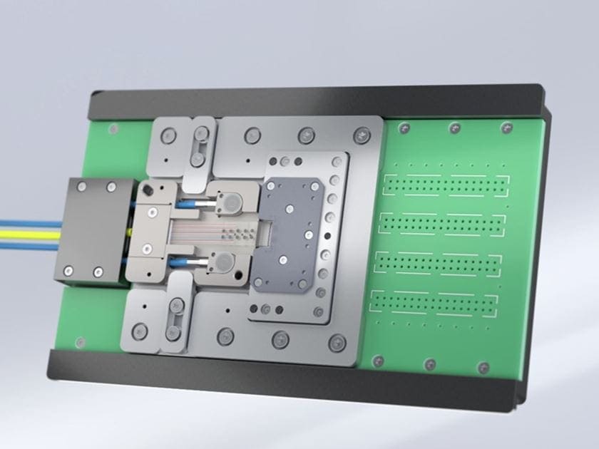
With the new UFO Probe® Vertical, Jenoptik is expanding its portfolio of probe cards for testing photonic integrated circuits (PICs) at wafer-level. Like the previous probe cards, the vertical version is based on the innovative UFO Probe® technology. This combines a novel optical concept with industry-proven needle technology in just one probe card and is also designed for use on standard wafer probers. Jenoptik is presenting this at this year's ECOC Exhibition 2023, a trade fair for optical communication, at the beginning of October in Glasgow, UK.
Time-saving parallel testing at high cycle rates
The consistent further development of the patented technology expands the possibilities of optical coupling and, with the new UFO Probe® Vertical version, enables parallel functional tests of optical as well as electrical components on chips using vertical needle technology from established test card manufacturers. This allows the user to couple up to 32 optical channels in parallel as standard – or more if required – without the need for active alignment.
This, as well as the time-saving parallel testing of optical and electrical components on wafers, makes the UFO Probe® Vertical particularly suitable for use in high-volume production. There, functional tests at wafer level are an important cost factor. With the help of the UFO Probe®, information about the functionality of the individual chips is available even before the subsequent process steps, such as dicing and packaging. Defective chips can thus be removed from the further process at an early stage. This increases the yield and reduces follow-up costs.
The UFO Probe® Vertical covers the entire wavelength range from 1260 to 1625 nanometers used in the telecommunications and data communications sector. Another new feature is the ability to provide/include polarization preservation for individual or all optical channels.
Powerful test solution for increased requirements
By incorporating the vertical needle technology, Jenoptik is responding to the increased market requirements, particularly with regard to co-packaged optics. Here, the trend is towards smaller chips with significantly more and therefore smaller and more densely packed electrical contacts. With the UFO Probe® Vertical, up to 6,000 bond pads with dimensions down to 35 microns can be contacted. Depending on the needle type, even more. Also, solder bumps and copper pillars are no problem. The smallest addressable pitch of the electrical contacts is in the range of 40 to 80 microns. In addition, the vertical probes provide a lower and more uniform contact resistance in the range of 0.2 to 1.0 ohms, depending on the probe type, while minimizing probe marks. These further developments ensure economical use in high-volume test scenarios and ATE operability.
Jenoptik will be presenting the UFO Probe® at the ECOC trade fair in Glasgow, Scotland, from October 2-4, 2023, at booth 736 as well as in an “EPIC TechWatch” presentation on site on October 4.
Images are available in the Jenoptik image database in the “Products” gallery.
About Jenoptik
Optical technologies are the basis of our business: Jenoptik is a global photonics group and comprises the two divisions Advanced Photonic Solutions and Smart Mobility Solutions. Our key markets primarily include semiconductor & electronics, life science & medical technology as well as smart mobility. In fiscal year 2022, Jenoptik generated revenue of 980.7 million euros. In fiscal year 2022, Jenoptik generated revenue of 980.7 million euros.
The Jenoptik Advanced Photonic Solutions division is a globally active OEM provider of system solutions and products based on photonic technologies. The company combines comprehensive expertise in optics, laser technology, digital image processing, optoelectronics and software. Under the TRIOPTICS brand, Jenoptik offers optical measurement and manufacturing systems for the quality control of lenses, objectives and camera modules. The customers of the Advanced Photonic Solutions division include leading plant and machine manufacturers as well as equipment manufacturers in areas such as semiconductors, laser material processing, medical technology & life science, industrial automation, automotive & mobility, security and also scientific institutes. The systems, modules and components used there help customers to optimally master their future challenges with the help of optical and photonic technologies.